Skip to content
How Submicron Particles Impact Semiconductor Yield

How Submicron Particles Impact Semiconductor Yield

Semiconductor manufacturing operates at scales where even the tiniest airborne particle or trace chemical vapor can destroy a circuit worth thousands of dollars. As device geometries push below 5 nanometers, maintaining pristine air quality inside cleanrooms has become one of the most critical factors in protecting yield and reliability.

This post explores how submicron particles and molecular contaminants infiltrate clean environments, the science behind HEPA and ULPA filtration, and how modern fabs are adopting smarter, more energy-efficient filtration systems.

From understanding the most penetrating particle size to applying multi-stage filtration strategies and IoT-based monitoring, we’ll break down how clean air translates directly into clean chips—and higher competitiveness in the semiconductor industry.

How submicron particles enter semiconductor cleanrooms

Submicron contamination enters through people, processes, and air systems. Managing these pathways keeps bays within their target ISO class and protects critical tools.

Sources: human activity, tool wear, chemicals, HVAC leaks

People shed skin flakes, hair fragments, and garment fibers—especially during gowning and material transfer. Tool motion and process steps generate fines from bearings, belts, wafer-handling components, and byproducts of etch, deposition, and CMP.

Non-rated wipes, swabs, liners, and packaging can release fibers and particulates. On the facility side, frame leaks, loose gaskets, unsealed penetrations, and weak pressure cascades allow bypass around final HEPA/ULPA stages. For the particle-size thresholds used in cleanroom classification, see the ISO 14644-1 cleanroom standard.

The role of recirculated air and unfiltered make-up air

Recirculation saves energy but can amplify a single breach: particles that escape upstream capture may persist through cycles and migrate across bays if airflow is non-uniform. Maintain adequate FFU density for downward laminar flow, protect finals with staged prefilters, and monitor differential pressure to time changeouts before shedding or imbalance occurs.

Ensure all make-up air is fully conditioned and filtered; verify seals with periodic leak/scan testing. For instrument calibration at submicrometer sizes, reference NIST sub-micrometer particle standards.

Common cleanroom classes and their particle limits (ISO 3–8)

ISO 14644-1 sets maximum concentrations per cubic meter at defined particle sizes (typically 0.1–5 µm). Advanced lithography and metrology zones often target ISO 4–5, while adjacent support areas run at ISO 6–8.

Tighter classes require higher air-change rates, efficient final filtration (HEPA/ULPA), and sufficient FFU coverage to prevent accumulation over critical surfaces. See official class limits in ISO 14644-1.

Measuring the impact — from defects to yield loss

Tiny particles translate directly into measurable yield loss. As line widths shrink, a single submicron particle can seed a “killer defect” that propagates through later layers and only surfaces at electrical test. Metrology programs quantify this link by tracking defect density (defects/cm²) versus die area to predict die-out and lot yield. For background on nanoscale contamination metrology, see NIST’s work on contamination control and particle standards used to calibrate counters and inspection tools: NIST sub-micrometer particle standards.

Typical yield loss attributed to particulate contamination

While the exact percentage varies by node and toolset, particulate excursions are a recurring component of non-systematic yield loss. Fabs monitor “defect paretos” to apportion losses among particles, process residue, and patterning errors.

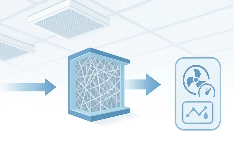
Particle-driven losses often spike after filter bypass, maintenance intrusions, or process drifts—hence the emphasis on continuous monitoring and rapid root-cause analysis.

Examples: pattern deformation, bridging, open circuits

Particles comparable to local critical dimensions distort photoresist profiles (pattern deformation), create conductive paths across adjacent lines (bridging), or block vias and trenches so metal fail to connect (opens).

During CMP, lodged particles can scratch or dish surfaces; during deposition/etch, they can shadow films, leaving voids or bumps that fail downstream reliability tests.

Cost implications: per-wafer and per-lot economics

Yield loss compounds quickly: fewer good die per wafer raises cost per functional chip and can push lots below release thresholds. Facilities model the full cost using standardized cost-of-ownership frameworks that include scrap, rework, downtime, and consumables. See the industry’s cost-of-ownership perspective in SEMI’s guidance: SEMI Cost of Ownership (COO) concepts.

A modest cut in particle-induced defect density can deliver outsized ROI by lifting die-per-wafer, stabilizing cycle time, and avoiding rework that consumes tool capacity and consumables.

The science behind filtration efficiency

Air filtration in semiconductor cleanrooms depends on how fibers capture particles across sizes and velocities.

Performance is expressed as fractional efficiency at different particle diameters, with special attention to the most penetrating particle size (MPPS), typically in the 0.1–0.3 µm range.

HEPA and ULPA filters: 99.97–99.9995% efficiencies

High-efficiency particulate air (HEPA) filters are rated to remove at least 99.97% of 0.3 µm particles, providing robust control for ISO 5–8 environments and many process bays.

Ultra-low penetration air (ULPA) filters extend performance to 99.999–99.9995% at or near the MPPS, supporting the tightest contamination budgets in advanced lithography and metrology zones.

Selecting between HEPA and ULPA hinges on the target ISO class, airflow rate, pressure drop allowance, and lifecycle cost.

Mechanisms: diffusion, interception, and electrostatic attraction

Diffusion dominates for the smallest particles. Submicron particles undergo random Brownian motion, wandering into fiber surfaces where they adhere.

Interception governs mid-sized particles that follow the airstream but pass within one particle radius of a fiber, resulting in contact and capture. Electrostatic attraction—present in charged (electret) media—enhances capture across a broad size range by pulling particles toward fibers via Coulombic forces.

Together, these mechanisms produce a characteristic U-shaped efficiency curve versus particle size.

Why smaller particles (0.1–0.3 µm) are hardest to capture

Particles in the 0.1–0.3 µm band sit in a “capture trough.” They are too small for strong inertial effects yet not small enough for diffusion to dominate, yielding the highest penetration through the media.

This is the MPPS region used to rate filters: if a filter meets its efficiency at the MPPS, it will perform as well or better for both larger and smaller particles under the same operating conditions.

Designing for this worst case—via proper media selection, adequate face velocity, and airtight seals—keeps actual delivered efficiency aligned with cleanroom yield goals.

Beyond particulates — the role of molecular contaminants (AMC)

Airborne molecular contamination consists of gases and vapors at ppb–ppt levels that never show up on particle counters but still damage devices and optics. In advanced fabs, AMCs originate from process chemicals, human outgassing, plastics and elastomers, FOUPs, and cleaning agents.

Unlike particles, these molecules diffuse everywhere, adsorb on surfaces, and can react during lithography, etch, deposition, or thermal steps, degrading yield without obvious clues on traditional environmental dashboards.

Why acid, base, and organic vapors also degrade yield

Acidic vapors such as HF, HCl, and SOx corrode copper and aluminum lines, shift contact resistance, and etch native oxides in unintended ways.

Basic species—especially ammonia—cause T-topping and footing in chemically amplified resists, disrupt photo-acid chemistry, and contribute to pattern collapse at tight pitches.

Organic vapors (solvents, organosiloxanes, and plasticizers) form molecular films on lenses, pellicles, and wafer surfaces, reducing optical transmission, seeding haze, and interfering with adhesion and etch selectivity.

These effects accumulate layer by layer, so even small excursions can translate into higher defect density, parametric drift, and latent reliability failures.

Complementary role of chemical filters (activated carbon, alumina)

AMC control relies on targeted chemisorption and adsorption stages placed where they intercept sources: at make-up air units, in recirculation paths, and within tool mini-environments.

Activated carbon beds capture a broad range of organics via physisorption; impregnated alumina and specialty media (e.g., permanganate, acid/base-specific chemisorbents) neutralize reactive acids and bases through irreversible reactions.

Effective designs pair particulate prefilters with AMC stages to protect media, minimize pressure drop, and extend life. Because breakthrough is chemistry-dependent, changeout timing should be based on upstream concentrations, bed kinetics, and continuous or periodic monitoring (e.g., TD-GC/MS, ion chromatography, or real-time AMC sensors), not on differential pressure alone.

Proper media selection, placement, and monitoring turn invisible molecules into a controlled variable—keeping optics clean, resists stable, and device parameters on target.

Strategies for maximum air purity

Achieving ultra-clean air requires layered filtration, stable airflow patterns, and disciplined maintenance.

The goal is to keep particle counts and molecular contaminants below class limits while minimizing energy and downtime.

Multi-stage filtration design: prefilter → HEPA → ULPA → AMC

Start with coarse and fine prefilters to capture larger dust and fibers, protecting final media from premature loading. Downstream, specify HEPA or ULPA finals to meet the target ISO class at the system’s most penetrating particle size.

Where airborne molecular contamination is a risk, add dedicated chemical stages—activated carbon for broad organics and impregnated alumina or specialty chemisorbents for acids and bases.

Place AMC beds so they treat make-up air and critical recirculation paths. Design housings with gasket compression control and scan-testable frames to eliminate bypass.

Airflow uniformity via FFUs and ceiling grids

Uniform, downward laminar flow prevents lateral transport and keeps contaminants away from wafer surfaces. Use a dense, evenly distributed array of fan filter units (FFUs) across the ceiling grid to maintain target face velocity and coverage over critical tools and aisles.

Balance supply and return to preserve pressure cascades between bays and chases. Avoid dead zones by coordinating FFU setpoints, tool exhaust, and return locations, and verify with smoke visualization or velocity mapping during commissioning and after layout changes.

Pressure-drop monitoring and replacement best practices

Track differential pressure across each filtration stage to spot loading trends early. Replace prefilters before they drive excessive ΔP; doing so extends HEPA/ULPA life and stabilizes airflow.

Establish alarms for rapid ΔP rise, correlate with particle counts and AMC data, and schedule changeouts during low-risk windows. After any media replacement, perform leak and scan testing, confirm gasket compression, and reverify airflow setpoints to restore the validated state.

Future trends in semiconductor air filtration

As semiconductor geometries continue to shrink and sustainability targets tighten, air filtration is evolving beyond traditional HEPA and ULPA performance.

The next generation of cleanroom systems integrates advanced media, lower energy consumption, and smart sensing to maintain purity with greater efficiency.

Nanofiber and composite filter media innovations

Nanofiber layers—ultrafine polymer fibers deposited onto conventional substrates—offer significantly higher capture efficiency with less resistance.

Their uniform pore structure enhances diffusion and interception for sub-0.1 µm particles while maintaining airflow uniformity. Composite filters that blend glass, synthetic, and nanofiber layers optimize both efficiency and dust-holding capacity, reducing changeout frequency. These materials also resist humidity and mechanical stress better than single-layer glass media, making them ideal for variable climate zones and high-cycle fabs.

Research and production data show nanofiber filters can achieve the same ISO class performance as thicker media while lowering initial pressure drop by up to 30%.

Energy-efficient low-ΔP filters

Energy consumption from cleanroom air handling can represent more than half of a fab’s total power use. Low-pressure-drop (low-ΔP) filters help curb fan energy without sacrificing purity.

Manufacturers are focusing on thinner pleats, optimized frame aerodynamics, and advanced fiber alignment to minimize flow resistance.

When combined with variable-speed FFUs and intelligent airflow zoning, these filters contribute to measurable sustainability gains under ISO 14001 and corporate carbon-reduction programs.

Smart cleanroom monitoring with IoT sensors

Digital transformation is reshaping how contamination control is managed. Smart filtration systems equipped with IoT sensors track differential pressure, airflow velocity, temperature, humidity, and particle counts in real time.

Connected dashboards can alert maintenance teams before filters overload, ensuring timely changeouts and preventing yield excursions. Predictive analytics refine service intervals based on actual data instead of fixed schedules.

Integration with building management systems (BMS) also enables dynamic fan control—automatically balancing energy savings with air cleanliness targets. As fabs advance toward Industry 4.0, smart filtration and sensor networks will become a cornerstone of yield assurance and operational efficiency.

Conclusion — clean air, clean chips, higher yields

Cleanroom air quality is a controllable driver of semiconductor yield. Particles and airborne molecular contaminants create killer defects, parametric drift, and latent reliability failures, but disciplined filtration, airflow control, and monitoring keep excursions rare and contained. Treat air purity as a production variable: specify the right media, validate performance in situ, and maintain it with data.

Key takeaways on contamination control ROI

  • Engineer a multi-stage stack: prefilter → HEPA/ULPA → AMC to protect tools and extend media life.

  • Design for uniform flow with adequate FFU density and verified pressure cascades to prevent lateral transport.

  • Monitor differential pressure, particle counts, and AMCs; replace on condition, not just on schedule.

  • After changeouts, leak/scan test and re-balance airflow to restore the validated state.

  • The payoff compounds: even small reductions in defect density lift die-per-wafer, stabilize cycle time, and free tool capacity, improving cost per good die.

Filtration quality and fab competitiveness

Filtration is not just compliance—it is a yield strategy. Fabs that pair low-ΔP, high-efficiency media with smart sensing cut energy use while holding tighter particle and AMC limits. This protects advanced lithography and metrology steps, reduces rework, and improves delivery predictability. In a market where nodes, uptime, and reliability define winners, clean air is an operational advantage that converts directly into margin and market share.

CleanLink filtration solutions for semiconductor industry

CleanLink delivers end-to-end air purity for fabs, from make-up air to tool mini-environments. Our portfolio combines low-ΔP media, tight leak integrity, and scan-testable housings to meet ISO 14644 targets while controlling energy and downtime.

Next article Why Air Filtration Matters in Cold Chain Food Transportation

Leave a comment

* Required fields